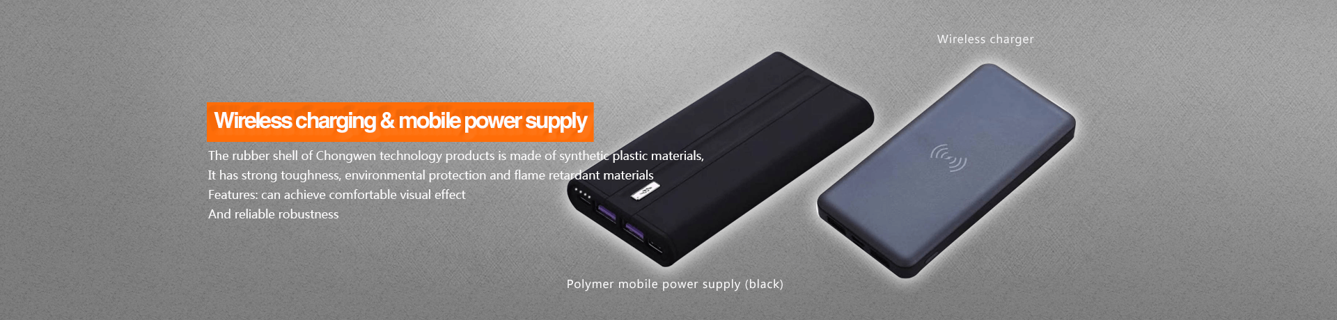
In the process of PCB design, it seems that a hole will not be left in the PCB design process. Today, let's talk about how to reduce the parasitic effect of vias in the vias design of high-speed PCB boards

1. The pin of power supply and ground should be drilled nearby. The shorter the lead between the via and the pin, the better, because they will lead to the increase of inductance. At the same time, the power and ground leads should be as thick as possible to reduce the impedance.
2. In other words, unnecessary vias should not be used as much as possible.
3. Using thinner PCB can reduce the two parasitic parameters of via.
4. Considering the cost and signal quality, the reasonable size of vias is selected. For example, for the design of 6-10 layer memory module PCB circuit board, it is better to select 10 / 20MIL (drilling / pad) via. For some high-density small size boards, you can also try to use 8 / 18mil vias. Under the current technical conditions, it is difficult to use the via with smaller size. For the via of power supply or ground wire, larger size can be considered to reduce the impedance.
5. Place some grounded vias near the vias on the signal layer to provide the nearest loop for the signal. Even a large number of redundant grounding vias can be placed on the PCB board. Of course, the design also needs to be flexible.
The via model discussed above is the case that each layer has pads. Sometimes, we can reduce or even remove the pads of some layers. Especially when the through-hole density is very high, it may lead to the formation of a broken slot in the copper layer to isolate the circuit. To solve this problem, in addition to moving the via position, we can also consider reducing the pad size of the via in the copper layer.

Why security misconceptions are threatening IoT devices in healthcare systems

Perception of user gestures in AR/VR scenes, and exposure of Apple's new "smart

From Chip to Cloud Internet of Things: A Decisive Step towards Web 3.0

Development status and opportunities and challenges of integrated circuit design