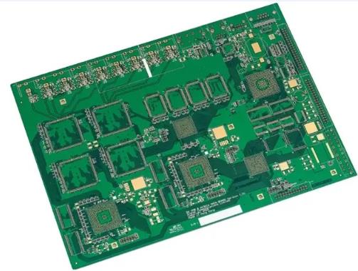
1、 Elements of PCB board
1. Working level
For printed circuit boards, the working level can be divided into six categories,
Signal layer
Internal plane layer
Mechanical layer is mainly used to place physical boundary and dimension information, which plays a corresponding prompt role. EDA software can provide 16 layers of mechanical layer.
The mask layer includes solder paste layer and solder mask layer. Solder paste layer is mainly used to paste surface mounted components on PCB, and solder mask layer is used to prevent soldering tin from being plated in places that should not be welded.
Silk screen layer draws the appearance outline and placement string of components on the top and bottom layers of PCB board. For example, the identification and nominal value of components, as well as the placement of the manufacturer's logo, production date, etc. At the same time, it is also the basis for the position of welding components on the printed circuit board. The function is to make the PCB board readable and facilitate the installation and maintenance of the circuit.
Other layers prohibit wiring layer keepoutlayer
Drillguidelayer
Drill drawing layer
Multi layer
2. Component packaging
It refers to the welding position and shape of the actual components when they are welded to the PCB board, including the overall dimensions of the actual components, the space occupied, the spacing between pins, etc.
Component packaging is a spatial function. Different components can have the same package, and components with the same function can have different packages. Therefore, the name and package form of components must be known at the same time when making PCB board.
(1) Component packaging classification
Through hole packaging (THT)
SMT surface mount technology
Another common classification method is from the package shape: SIP single in line package
Dip dip package
PLCC plastic lead chip carrier package
PQFP plastic quad flat package
SOP small size package
TSOP thin small size package
PPGA plastic needle grid array packaging
PBGA plastic ball grid array packaging
CSP chip level package
(2) Component package number
Number of pins + pin size + component type
For example, axial-0.3dip14rad0.1rb7.6-15, etc.
(3) copper film wire refers to the wire connecting the components on PCB, which is the most important part in PCB design. For the copper film conductor of printed circuit board, the wire width and wire spacing are important indicators to measure the copper film conductor. Whether the size of these two aspects is reasonable will directly affect whether the components can realize the correct connection between the circuit.
Principle of PCB routing:
Wiring length: try to run short wires, especially for small signal circuits. The shorter the line, the smaller the resistance and the smaller the interference.
Line shape: when the signal line on the same layer changes direction, it should take 135 ° oblique line or arc to avoid 90 ° corner.
Wiring width and spacing: in PCB design, the width of PCB lines with the same network properties should be as consistent as possible, which is conducive to impedance matching.
Generally, the signal line width is 0.2-0.3mm, (10mil)
The power line is generally 1.2-2.5mm. In the range of allowable conditions, the width of power supply and ground wire should be widened as far as possible. The best way is to make the ground wire more than the power line width. The relationship between them is: ground wire > power line > signal line
Spacing requirements of pad, wire and through hole
PADandVIA :≥0.3mm(12mil)
PADandPAD :≥0.3mm(12mil)
PADandTRACK :≥0.3mm(12mil)
TRACKandTRACK :≥0.3mm(12mil)
When the density is high:
PADandVIA :≥0.254mm(10mil)
PADandPAD :≥0.254mm(10mil)
PADandTRACK :≥ 0.254mm(10mil)
TRACKandTRACK :≥ 0.254mm(10mil)
4. Pads and vias
Pin drilling diameter = pin diameter + (10 ~ 30mil)
Pad diameter of pin = drilling diameter + 18mil
#PCB layout principle
1、
According to the structure diagram, the size of the board and frame is set, and the installation holes, connectors and other devices that need to be positioned are arranged according to the structural elements, and these devices are endowed with immovable property. The dimension shall be marked according to the requirements of process design specification.
Two
According to the structure diagram and the clamping edge required in production and processing, the no wiring area and no layout area of printed circuit board are set. According to the special requirements of some components, no wiring area is set.
Three
Considering PCB performance and machining efficiency, the processing flow is selected.
The optimal order of processing technology is as follows: single side mounting on component surface, component surface mounting and plug mixing (one-time wave forming of component surface inserting and welding surface mounting), double-sided mounting, component surface mounting, and welding surface mounting.
Four
Basic principles of layout operation
A. According to the layout principle of "first big and then small, first difficult and then easy", the important unit circuit and core components should be given priority
B. The layout should refer to the principle block diagram and arrange the main components according to the main signal flow direction of the single board
C. The layout shall meet the following requirements as far as possible: the total wiring shall be as short as possible, and the key signal line shall be the shortest; high voltage and high current signals shall be completely separated from small current and low voltage weak signals; analog signals shall be separated from digital signals; high frequency signals shall be separated from low frequency signals; high frequency components shall be separated from each other